Project Overview
An STM32-based development board designed to begin your Embedded Systems journey.
Introducing the STM32PlayBoard. As the name suggests, the main object of developing this board is to expand my knowledge and provide an entry gate for others to learn Embedded Systems with a well-known and documented microcontroller by STMicroelectronics. This project opens the door to immersive learning experiences and practical experimentation.
Resources: STM32PlayBoard’s GitHub Repository
Why I designed STM23PlayBoard
I pictured a compact design for the STM32PlayBoard that prioritized accessibility to a wide range of communication protocols while offering dedicated pins for ADC, timers, and some general-purpose I/Os.
This careful pin allocation aimed to balance versatility, functionality, and ease in PCB designing. By providing exposure to commonly used communication interfaces and essential GPIO options, the board becomes an adaptable platform for various applications.
Additionally, the compact nature of the design wasn’t just about efficient use of space; it also served a practical purpose. I aimed to create a development board that could seamlessly integrate into my other projects as a convenient replacement. This design approach allows for easy adaptability across different projects, simplifying development and minimizing the need for significant redesigns.
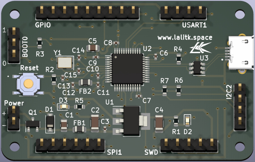
System Architecture
Component Selection
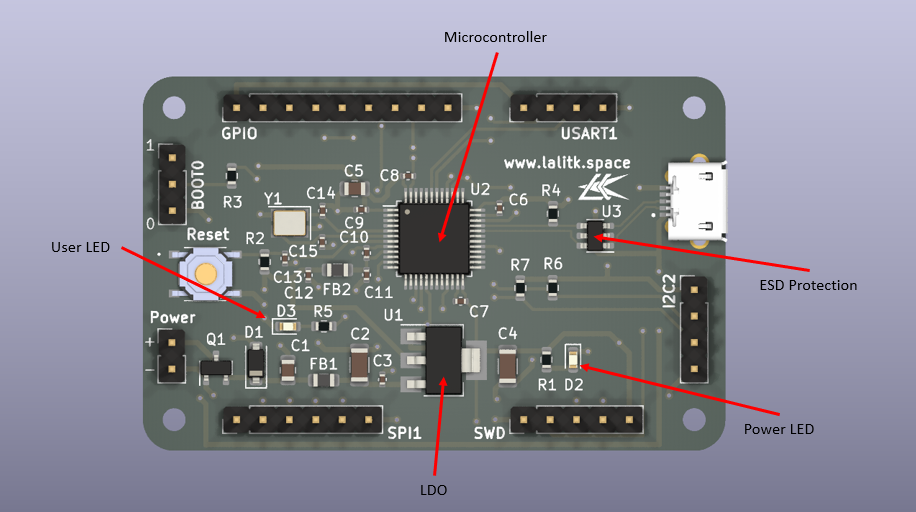
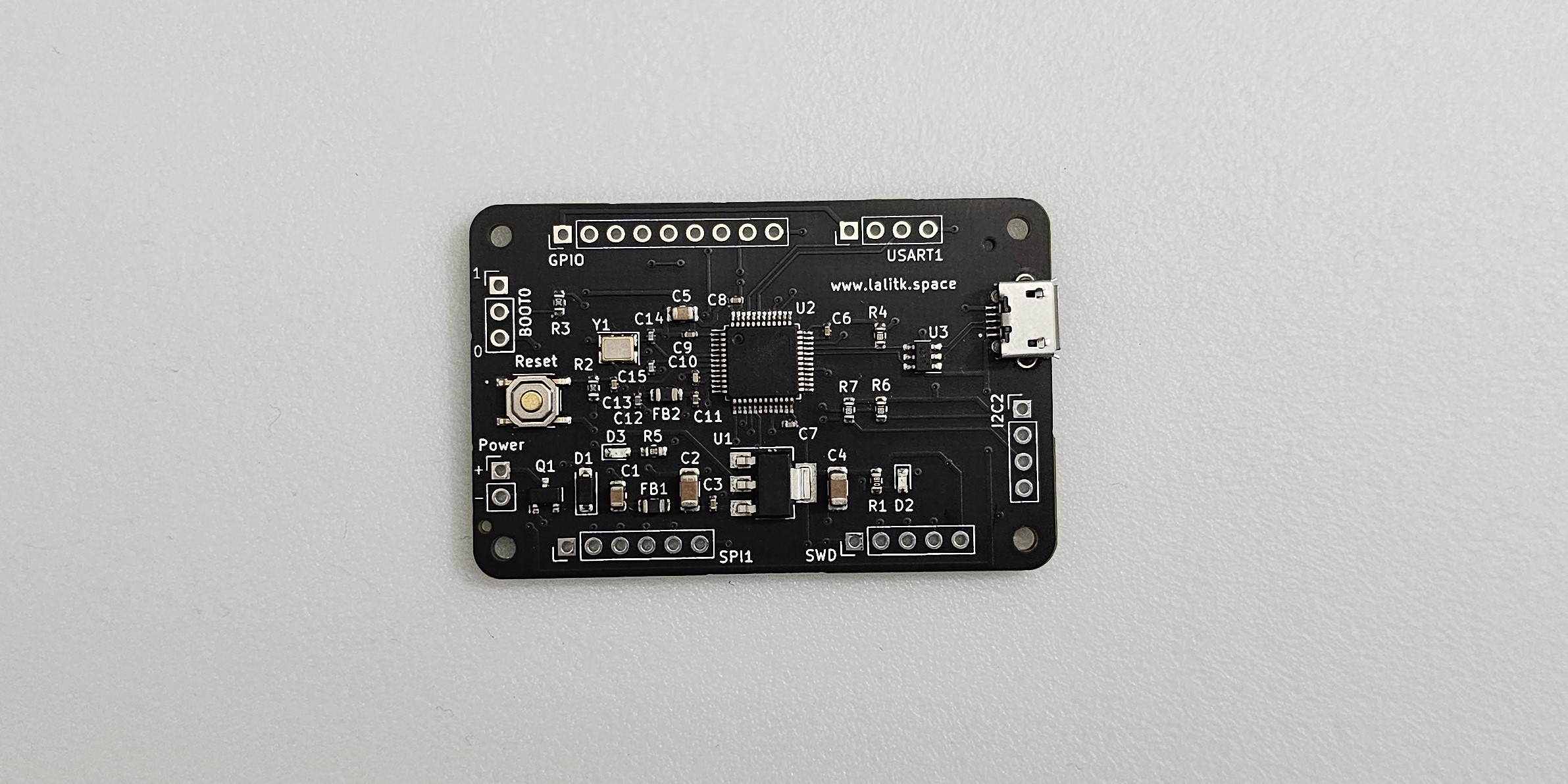
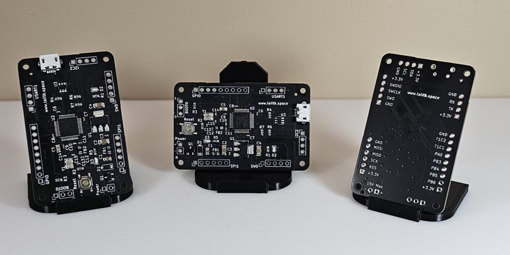
Microcontroller:
- The board’s core is an STM32F103C8T6 microcontroller from STMicroelectronics, running with a 16MHz High-Speed External Oscillator.
- Board has a configurable BOOT0 for different operational modes.
- A physical reset button for manually resetting the board.
Power Supply:
- The board can be powered by an external voltage supply and through Micro B USB. They are reverse polarity protected and can both coexist.
- The voltage regulation is accomplished using AMS1117-3.3 linear voltage regulator from Advanced Monolithic Systems. Since the main component on the board is the main microcontroller IC, I went with this standard, less expensive, and easily available LDO.
- The maximum voltage that can be provided externally is 18V, and the maximum drop-out voltage of this LDO is 1.2V at 1A. We are going to be far from this current consumption using this board.
- The Silkscreen on the back side of the PCB shows 15V is just an additional safety measure (not to exceed 15V even though up to 18V is acceptable).
USB:
- The board supports USB 2.0 full-speed interface using a Micro B connector.
- The board provides ESD protection on USB using USBLC6 IC from STMicroelectronics.
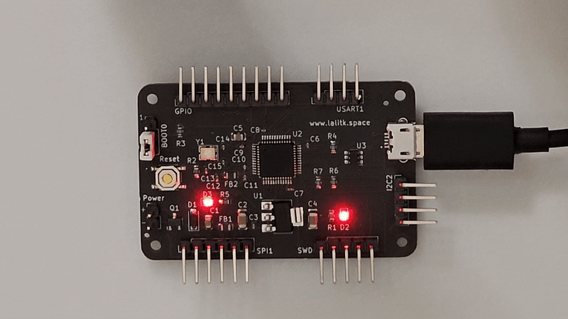
Onboard LEDs:
- D3 is onboard status LED and is connected to pin PA1. The cathode of the LED is permanent ground.
- D2 is the Power LED indicating a healthy power supply.
Design and Schematics
Schematics:
Link to -> Schematics
Board Layout Considerations:
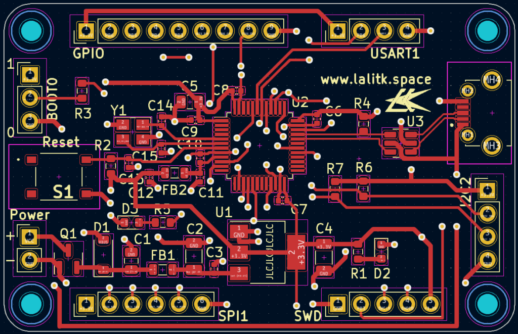
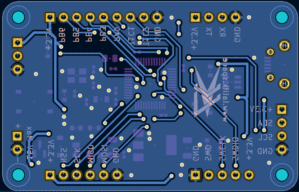
- The PCB is two layered board. The reason for being two layers is I wanted to go with a simple board design, which also minimizes the production cost.
- The entire bottom layer of the board is grounded, and the Top layer is the signals layer.
- A wide trace of 0.5mm is for power, and a 0.3mm trace is for signals.
- The board dimensions are 56x36mm.
Front Copper:
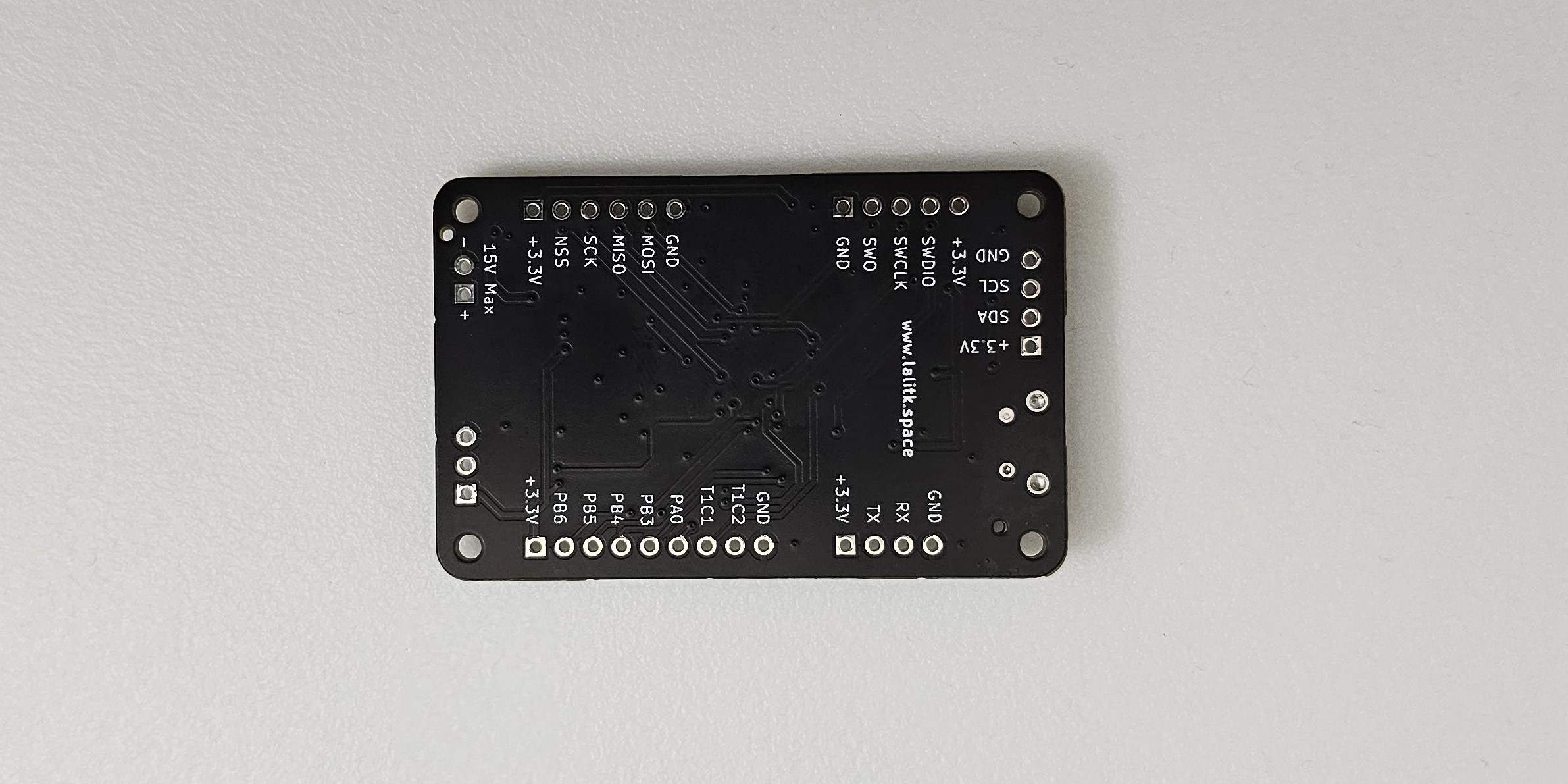
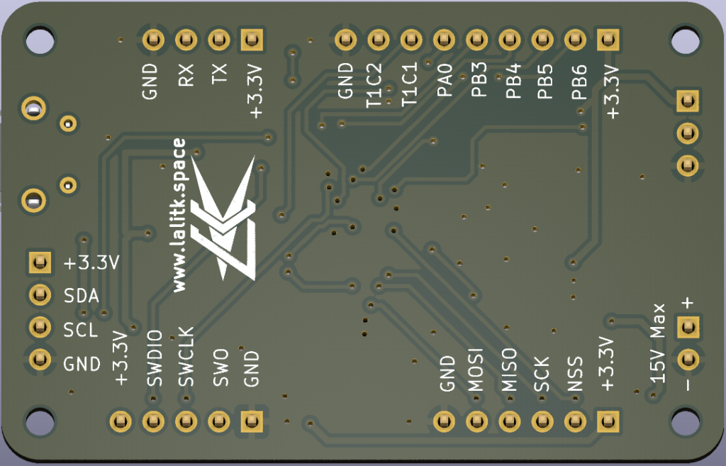
Back Copper
Interfacing and Capabilities
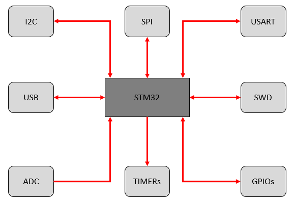
- This board functions as a development board with GPIO and communication protocols exposed. The board exposes:
- 1 SPI connection (SPI1)
- 1 I2C connection (I2C2)
- 1 USART connection (USART1)
- SWD for programming and debugging
- 1 ADC (ADC1_IN0)
- 2 timers (TIM1_CH1 and TIM1_CH2)
- 4 GPIOs from Port B (PB3, PB4, PB5, PB6)
- An onboard LED on pin PA1
- The voltage level for all the pins is 3.3V. And for interfacing with other 5V level compatible boards (for example, Arduino), a logic level shifter/converter is required.
Software Development
The board can be programmed using an external ST-Link programmer via the SWD interface.
Technical Specification
| Input Voltages | Max Values |
|---|---|
|
Through USB connector |
5V |
|
Through power connector |
18V |
| GPIO Tolerances | Max Values |
|---|---|
|
All pins |
3.3V |
| Memories | Size |
|---|---|
|
FLASH |
64 Kbytes |
|
SRAM |
20 Kbytes |
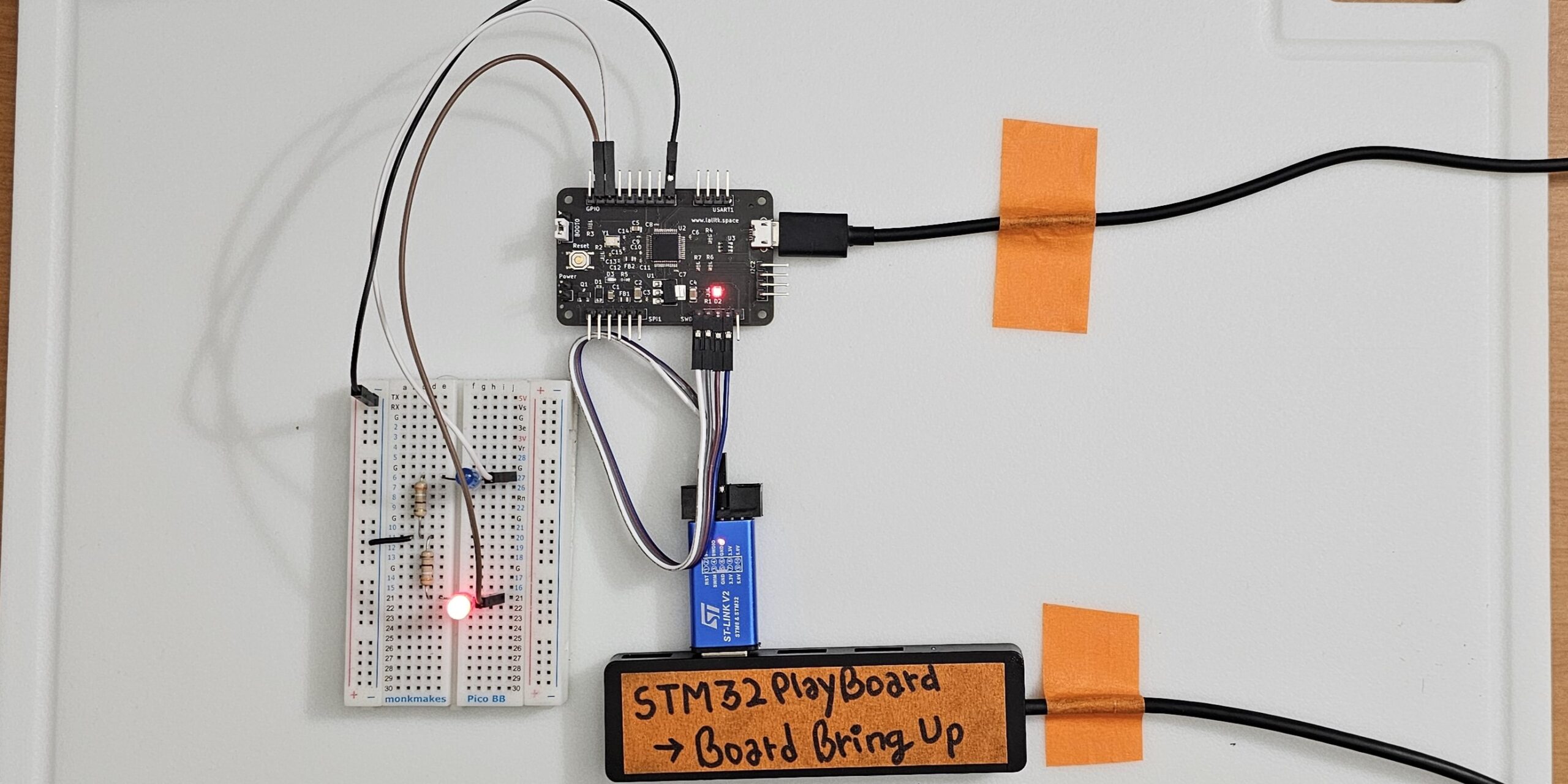
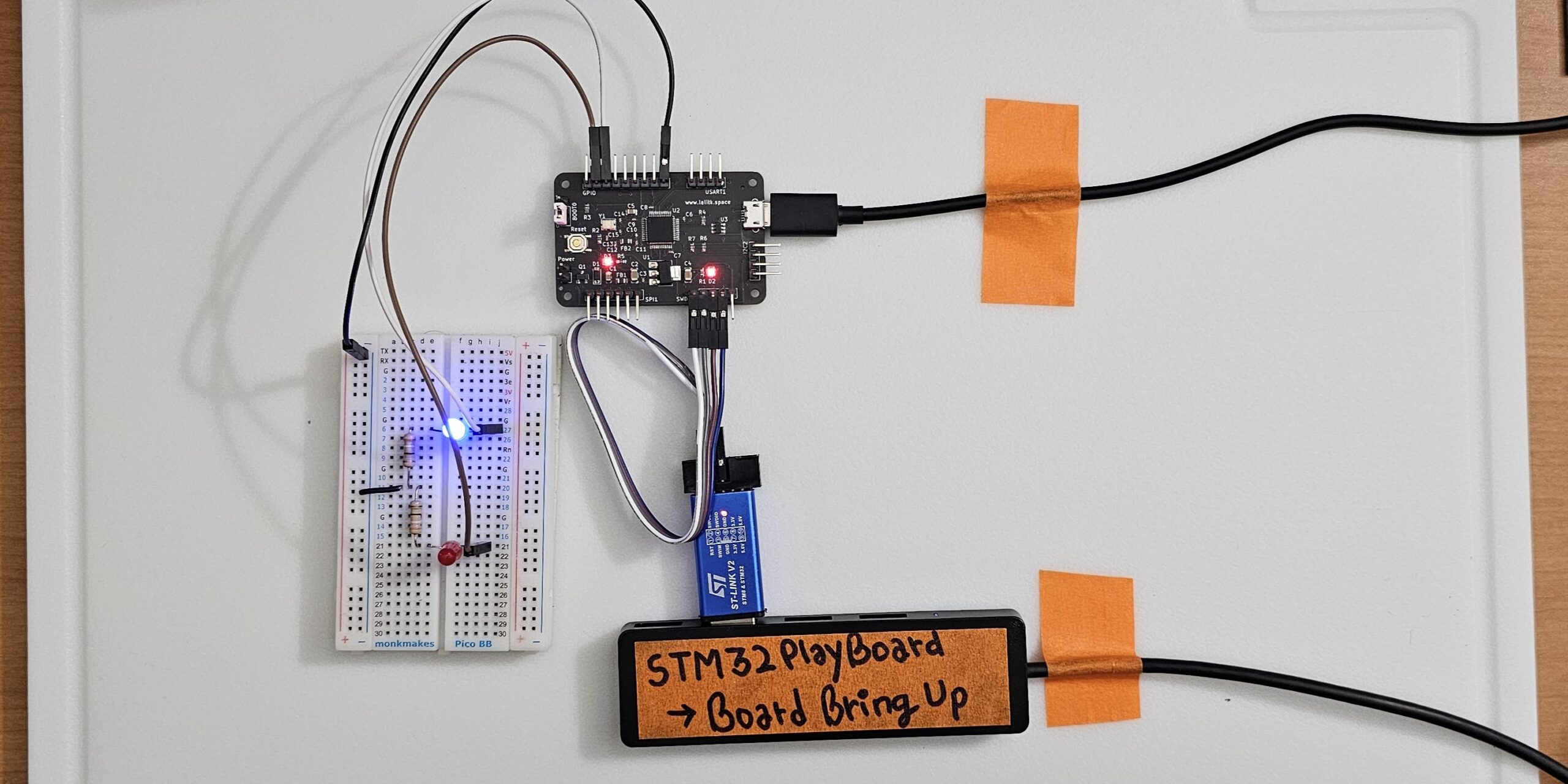
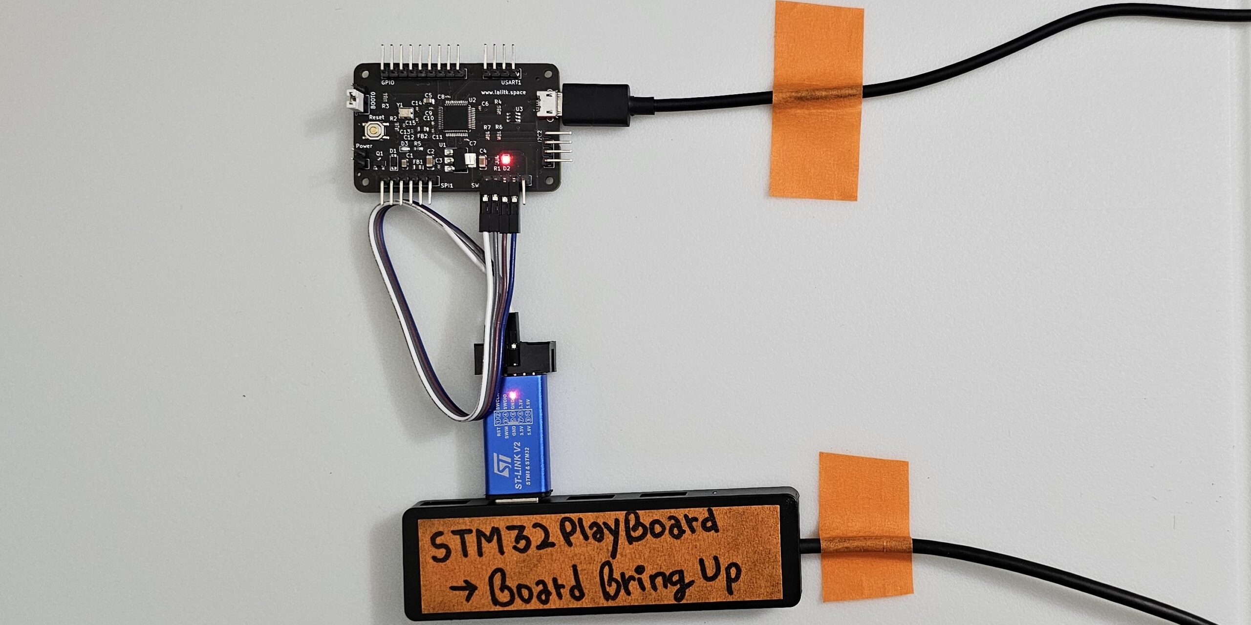
Board Bring-Up
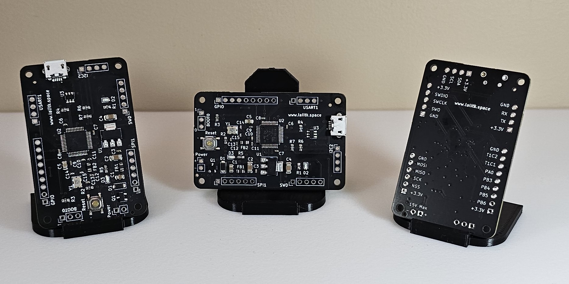
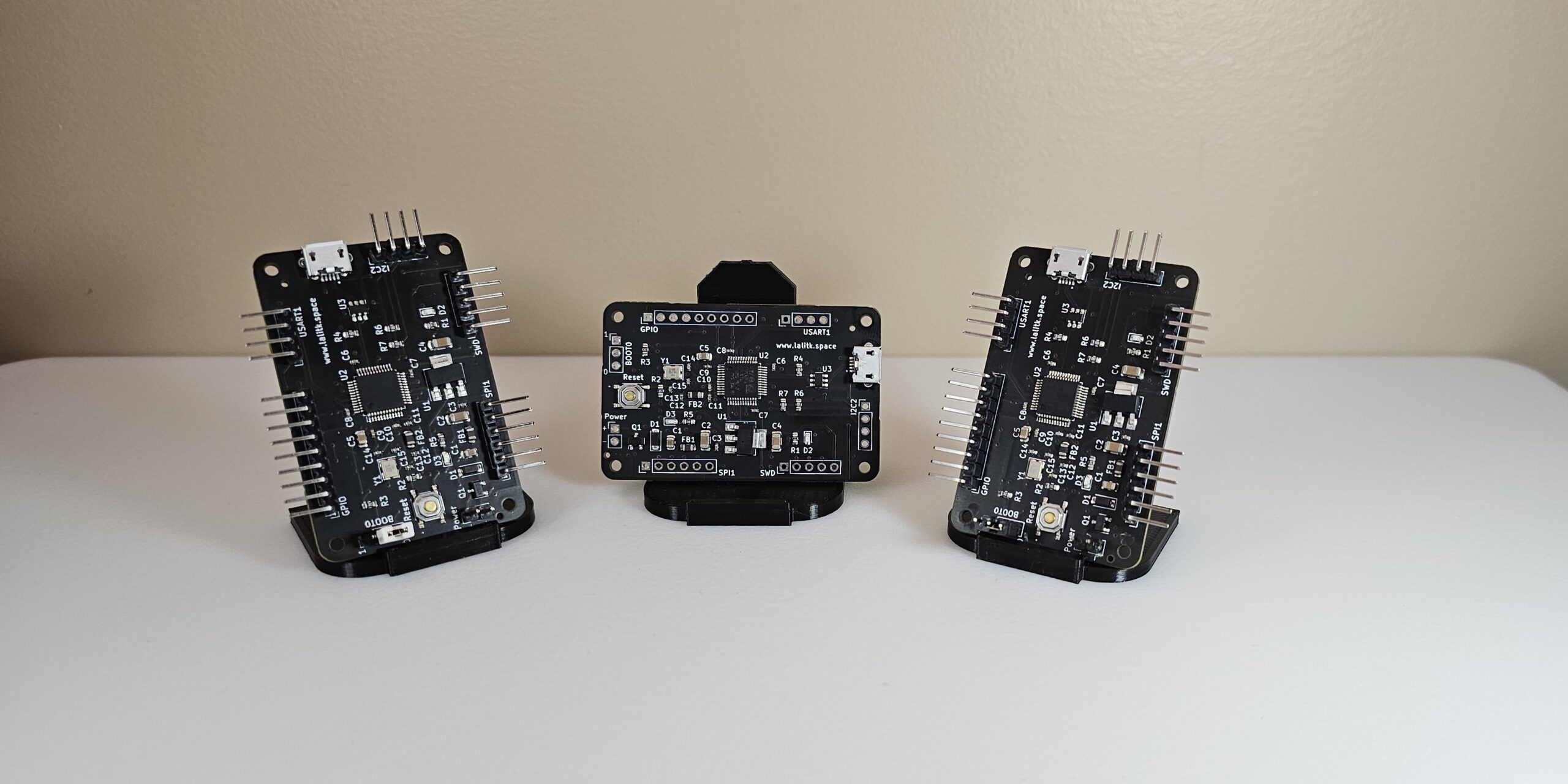
Manufactured and Assembled Board
Powering Up and Blinking Onboard LED
| Exposed Peripherals | Connected to |
|---|---|
|
I2C2_SDA |
PB11 |
|
I2C2_SCL |
PB10 |
|
USART1_RX |
PB7 |
|
USART1_TX |
PB8 |
|
SPI1_NSS |
PA4 |
|
SPI1_SCK |
PA5 |
|
SPI1_MISO |
PA6 |
|
SPI1_MOSI |
PA7
|
|
Status LED D3 |
PA1 |
|
ADC1_IN0 |
PA0 |
|
TIM1_CH1 |
PA8 |
|
TIM1_CH2 |
PA9 |
|
GPIO1 (USART1 TX) |
PB6 |
|
GPIO2 |
PB5 |
|
GPIO3 |
PB4 |
|
GPIO4 (SWO) |
PB3 |
My learnings
Throughout the development of this board, I discovered a lot regarding designing a PCB with a microcontroller on it and various design practices like decoupling and bulk capacitors. I also wanted to learn to program a STMicroelectronics microcontroller using an external programmer, and I achieved this using this board.
As per software development skills, I am writing my drivers for various peripherals and example codes for this board, which are available on my GitHub repository.
Foundations for the Future
Keeping this project as a base, I would like to design and develop another STM32-based development board with a different, more powerful microcontroller with various onboard peripherals like FLASH memory and some onboard sensors communicating with the main IC using multiple communication protocols.
Gallery